Equipment
» Computational Resources
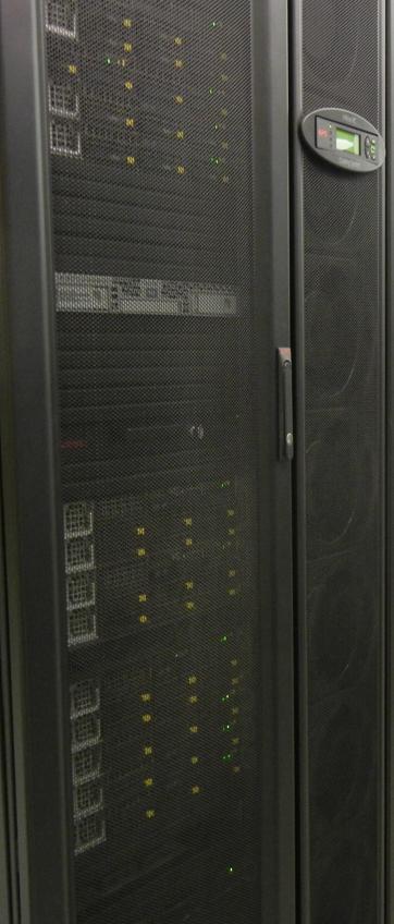
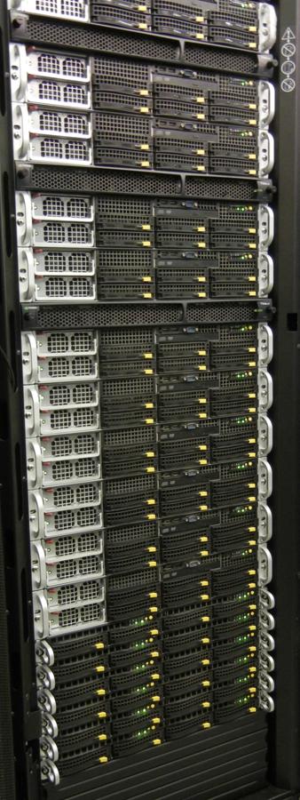
Aryabhata : High Performance Computing Cluster
 |
|
 |
» Experimental Resources
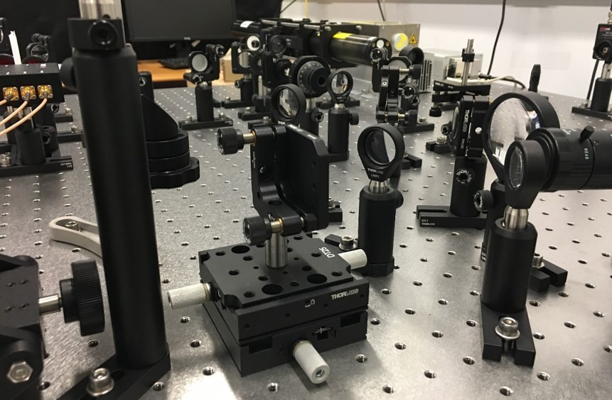
Time-domain Thermo-reflectance Method
The nanosecond thermoreflectance method is a non-contact and non-destructive pump-probe optical technique that allows for simultaneous heating and probing of a sample surface and is used to estimate the thermal properties of thin films and/or the underlying substrate. A typical sample geometry consists of a substrate (i.e., Si) coated with a thin metal transducer film (~100 nm) deposited using physical vapor deposition. In the thermoreflectance measurements, a pulsed pump laser (10-100 KHz) causes a temperature rise and decay at the surface of the metal transducer film. Heat diffusion through the sample is monitored through the change in the thermoreflectance signal using a probe laser. The decay of the surface temperature is strongly influenced by local thermal resistances below the surface. The experimental data is fit to a thermal model in order to extract thermal properties of interest (e.g., metal-substrate thermal boundary resistance, substrate thermal conductivity).
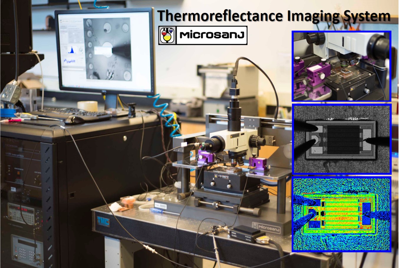
Microsanj Thermo-reflectance Camera
The operation of Microsanj thermal imaging system is based on non-invasive optical thermo-reflectance technique. This technique utilizes the relative change in the surface reflectivity of the sample due to the change in its temperature. It can be used for ultra-fast measurement of temperature distribution of the electronic materials and devices which will help in thermal design, defects and failure analysis. The system has the capability for time-sensitive hot-spot detection and reliability analysis with 300 nm spatial resolution, 100 ns temporal resolution and thermal resolution of 0.5 °C. Due to its superior spatial and temporal resolution, the system can be very useful for the thermal analysis of increasingly smaller microelectronic and optoelectronic materials and devices. The system serves as a great tool for advanced semiconductor device research, design, and development.
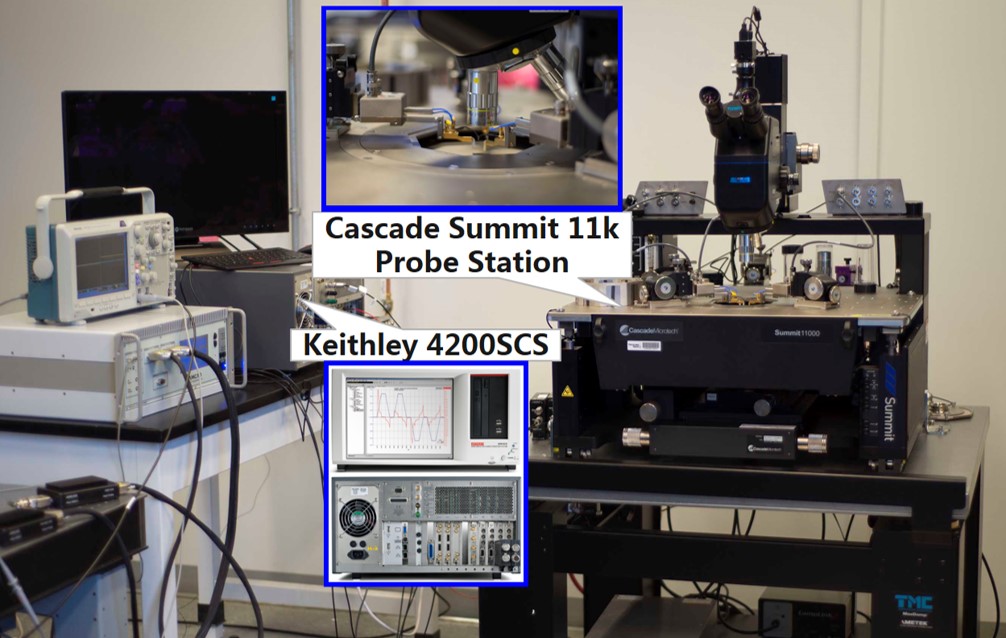
Cascade Summit 11k
Cascade Summit 11k is an automated probe system. It allows us to access the full range of test instrument for wafers as large as 200mm in application such as RF/Microwave, device characterization, wafer level reliability, e-test, modeling, or yield enhancement etc. Measurement accuracy can be reached by minimizing AC and spectral noise with effective shielding capability. Manual 3-axis stage enables fast, accurate ‘hands on’ wafer positioning with ergonomic controls. The temperature of platform can go as high as 300 C to meet thermal needs as well as high temperature stability enhancement. It is also very easy to configure with choices of measurement performance, chuck size, thermal range and microscope options.
Keithely 4200 SCS
Keithely 4200 SCS is a semiconductor characterization system which provides I-V, pulsed I-V and C-V characterization of semiconductor devices and test structures. It contains basic configurations and capabilities of the Source-Measure Units (SMUs), preamps, pulse generator card, Digital Storage Oscilloscope, and Capacitance-Voltage Units (CVUs) that are connected to Devices Under Test (DUTs). Tests are easily and quickly configured and executed from multiple software such as the Keithley Interactive Test Environment (KITE), KXCI, KCON, KPulse etc. Advanced digital sweep parameter analyzer combines speed and accuracy for deep sub-micron characterization. Multiple cable plans are provided for connection between 4200 SCS and Summit 11k to ensure high speed and high accuracy tests of our FETs as well as other nano-electronic device as needed.
Device fabrication and characterization are performed at Georgia Tech Institute for Electronics and Nanotechnology. This research facility includes:
E-beam Nanolightography, Nanoimprinting, Atomic layer Deposition, Plasma Enhanced Chemical Vapor Deposition, PVD RF Sputterer, Electron Beam Evaporator, Filament Evaporator, ICP and Plasma Reactive Ion Etch Chambers, Tristar Nitride Furnaces, Wet and Dry oxidation, Scanning Electron Microscope, Auto-load and Manual Spin Coater, Spin Develop Station, Mask Aligner/UV Exposure Tool, Automated Dicing Saw, Polishing and Lapping Stations, Wire Bonders, Dark Room Facility for Mask Generation, RF & DC Magnetron Sputtering Systems. Metrology tools include AFM, KLA tencor Profilometer, Wollam Ellipsometer, Nanospec Refractometer.