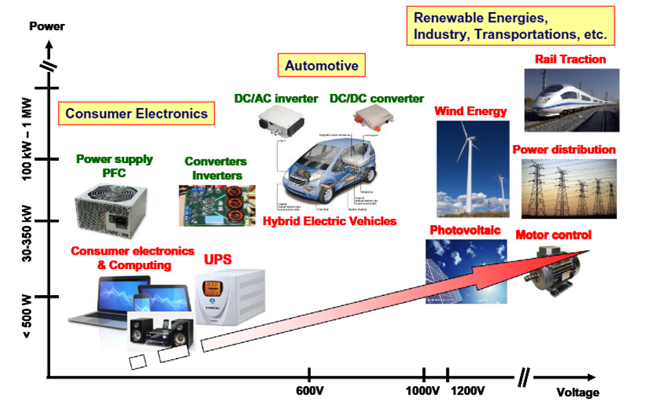
Projects
|
(a) Isometric view of a BMW i3 125 kW permanent magnet synchronous motor, (b) computational domain for CFD/HT simulation. at High Electric Field
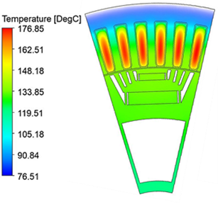
 Temperature distribution in a conventional jacket cooled of a BMW i3 motor. at High Electric Field
 |
We focus on thermal management of devices at different length scales, e.g., development of heat spreader or application of thermo-electrics for hot spot thermal management on chips in portable electronic devices and two-phase thermal management of electric motors. In the last decade, we have witnessed an increasing interest to move from traditional fuel-powered transportation to electrical motor driven low carbon emission transportation i.e., electric vehicle (EV), and hybrid electric vehicle (HEV). Electric motor along with battery and inverter are commonly known as the heart of the EVs. High internal heat generation and inefficient heat removal often limit the operational reliability, and longevity of the electric motor. The state-of-the-art (SOA) single-phase liquid cooling become inadequate for the compact motor because of the irregular geometry and non-uniform heat generation. Advanced thermal management of electric motors is critical for the next generation EV design. Our research focuses on the development of the advanced latent heat driven two-phase thermal management for electric motors. We emphasis on developing coupled electro-magnetics and computational fluid dynamics-heat transfer (CFD-HT) model to characterize the effectiveness of our proposed two-phase thermal management system. We demonstrate the viability of the new thermal management framework for three times higher power and torque density of a significantly smaller motor volume compared to the conventional electric motor. » More Details |
Multi-scale Transport Modeling of Nanoscale Materials and Their Interfaces
|
As electronic device size continues to scale down and power density continues to increase, one of the major challenges we face is how to manage the resulting heat fluxes. The relevant length scale of modern electronic devices is well into the nanoscale, where thermal transport phenomena is sensitive to material and device structure at the atomic level. The accurate description of thermal transport phenomena in these devices is a challenging task: Fourier’s law of heat conduction fails at the nanoscale and atomistic simulation methods are required to accurately capture the thermal transport physics. We focus on exploring thermal transport physics in novel electronic device materials and across material interfaces using atomistic simulation methods such as density functional theory (DFT), atomistic Green's function method (AGF), and Molecular Dynamics (MD). We use machine learning (ML) techniques to develop ML-based interatomic potentials for fast and accurate MD simulations and materials discovery. With these techniques, we study complex thermal transport phenomena such as the influence of defects and doping on thermal conductivity and the effects of lattice stacking configurations on phonon transmission across material interfaces. » More Details |
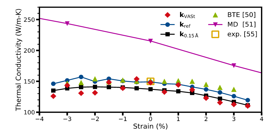 Thermal conductivity of silicon as a function of isotropic strain predicted using a newly developed Voxelized Atomic Structure (VASt) potentials. |
|
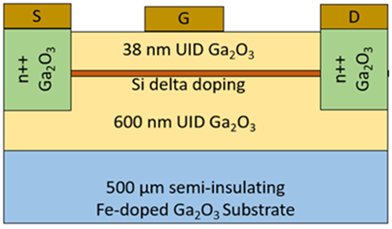
A schematic of the Ga2O3 MESFET Potential applications of Ga2O3 in power electronics (Source: F. Roccaforte et al. Microelec. Engg. Vol 187–188, 5 Feb 2018, Pg 66-77)
|
Wide bandgap (WBG) materials (SiC, GaN) have significant advantage over narrow bandgap materials such as Si, GaAs for Power and RF electronics applications. As WBG materials based technology mature, a new class of materials, known as ultra-wide bandgap materials, with even wider band gap than SiC and GaN is
emerging. Gallium oxide is one of the most promising candidates in this class. Its ultra-wide bandgap can help achieve even higher breakdown voltages and switching efficiency. Low thermal conductivity of β-Ga2O3 leads to self-heating in its FETs and heat dissipation poses a significant challenge for viability
of these devices. Accurate prediction of the electrical and thermal characteristics of these devices is needed for efficient thermal management and device design. We investigate the electro-thermal transport in β-Ga2O3 based field effect transistors (FETs) using a combination of modeling and metrology techniques.
|
Flexible Electronics
|
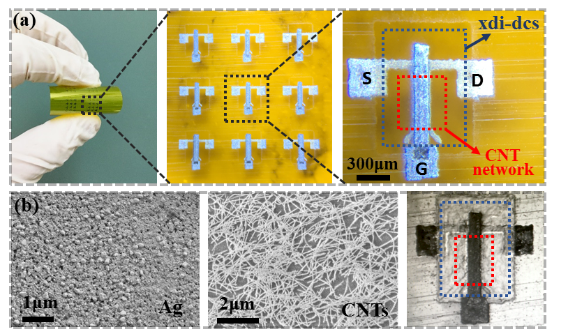
The field of printed electronics has been gaining popularity and maturity in the last decade. The promise of extremely-low-priced electronic components and sensors platforms, enabled by printing technologies such inkjet printing (IJP) or aerosol jet printing (AJP), seems attainable at large
scales in the near future. This revolution has been possible not only because of the advances in additive technologies, but also the availability of different solutions (inks) that contain conductors, semiconductors and dielectric materials such as silver nanoparticles (Ag), carbon nanotubes
(CNTs), hexagonal boron nitride flakes (hBN). AJP has advantages since it can use inks whose viscosities are in the range of 1 to 1000 cP, and resolution in the range of 10 to 20 um can be achieved.
Our group have developed CNT FET’s with low threshold voltage (~ 5V) by carefully printing each layer of the transistor. The electrodes were fabricated with silver nanoparticle-based ink. For the semiconducting layer, 99.9% CNT-based ink was used. The dielectric layer is made of xdi-dcs, a
commercially available dielectric ink, which is a blend of mixture of poly(vinylphenol)/poly (methylsilsesquioxane). Controlling the ingredients of the different inks allows for an optimized performance of the devices.
|
|