Projects
>
Ultra-Wide Bandgap Materials and Devices for Power and RF Electronics
|
Electrothermal modeling: We aim to develop 2-D electrothermal model for β-Ga2O3 based FETs using Synopsys TCAD Sentaurus. We study the effect of bias condition and power settings on Joule heat generation and temperature distribution in the device. We can couple TCAD Sentaurus with Ansys Fluent/COMSOL to study effectiveness of various device-level thermal management for future device designs. 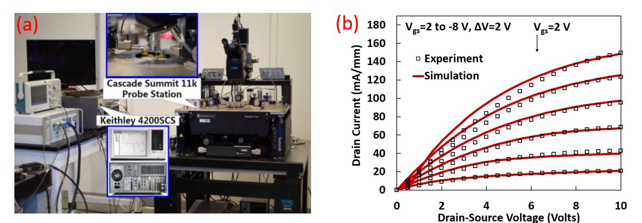 Fig. 1. (a) Keithley 4200-Semicodnuctor Characterization System and (b) Comparison of modeling and measurement results.
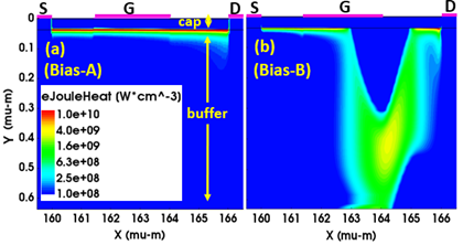 Fig. 2. Electron Joule heat density profiles in the device when power =1.16 W/mm with (a) Bias-A: Vds=8.3 V and Vgs=2 V (b) Bias-B: Vds=25 V and Vgs=-6 V. Even though power dissipation is same in both the cases but the electron Joule heat profiles are significantly different.
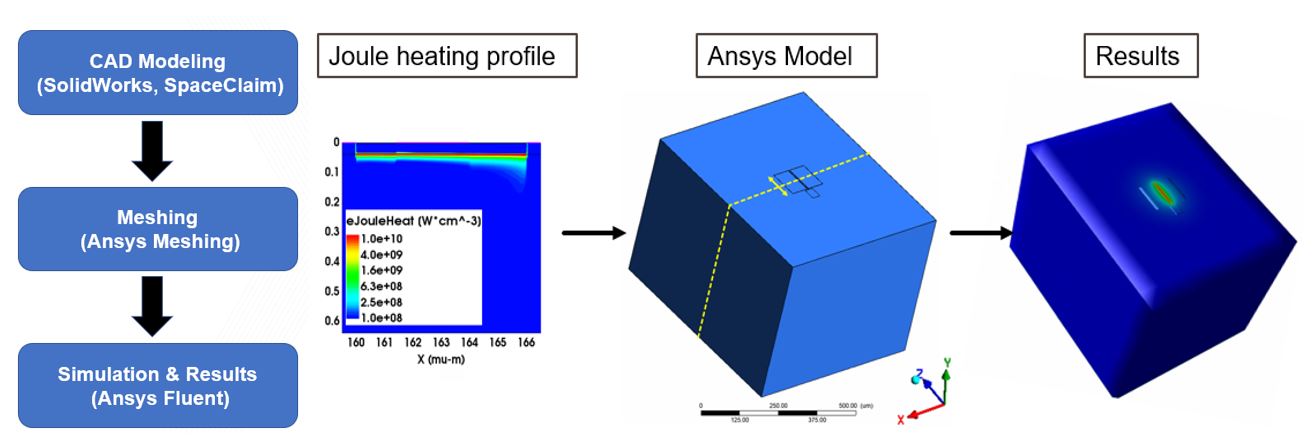 Fig. 3. Procedure of 3-D thermal modeling in Ansys Fluent.
Ultrafast Thermoreflectance Imaging: We use thermoreflectance imaging to measure the spatial and temporal variation with nanoscale resolution of temperature β-Ga2O3 devices. The Microsanj thermoreflectance system NT210B with piezoelectric stage is used for thermoreflectance imaging. We measure the temperature contours on source, drain and gate pads and estimated peak temperature at different bias conditions, and calculate thermal time constants, which can be used to predict their transient thermal behavior and compact electrothermal modeling. 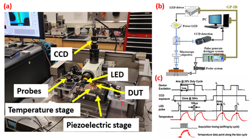 Fig. 4 Microsanj thermoreflectance imaging system. (a) Experimental setup (b) Depiction of different components of the setup. (c) Timing control during transient measurements.
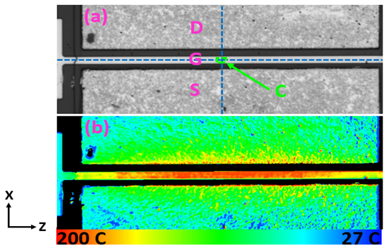 Fig. 5. (a) A CCD image of the device using 100x objective, (b) Temperature contours of the electrodes at power = 2.56 W/mm obtained from thermoreflectance imaging.
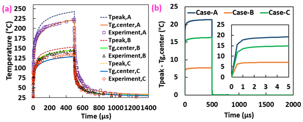 Fig. 6. Transient thermal measurements at the gate-center ‘C’, which is marked in Fig. 5(a). Measured and computed temperatures for a pulse width of 500 μs and 25% duty cycle (i.e., pulse period is 2 ms) for (a) Case-A: power = 3.25 W/mm (Vgs = 2 V; Vds= 20 V), Case-B: power = 2.04 W/mm (Vgs = 2 V; Vds = 13.3 V), and Case-C: power = 1.85 W/mm (Vgs = -2 V; Vds = 20 V). (b) difference between peak temperature and gate center temperature with time for Case-A, B and C.
Phonon Transport: We study phonon transport in β-Ga2O3 thin films and FETs using non-gray Boltzmann Transport Equations (BTE). This work helps in understanding the mechanism of phonon transport in the β-Ga2O3 FETs and provide insights for the future design of β-Ga2O3-based electronic devices. It is expected that the BTE model can provide a much more accurate temperature distribution compared to the Fourier model which would significantly under predict the hot spot temperature.
Relevant Publications |
|
|
Funding: NSF
|
|
