Projects >
Electro-Thermal Transport in Flexible Electronics
|
Carbon nanotubes (CNTs) are promising and useful materials for several applications due to their good thermal, electrical, optical and mechanical properties. Many studies have been performed in the past decade to explore and develop devices which could leverage the excellent properties of individual CNTs and their two- and three-dimensional (2D and 3D) networks. In particular, CNT network thin film transistors (CN-TFTs) have been explored for a wide range of applications such as flexible displays, sensors, antennas, etc. CNT networks are typically supported on thermally insulating substrates such as glass or plastics, which have very low thermal conductivity and where the excessive self-heating in CN-TFTs under high field operations can lead to the breakdown of these devices. In addition, the variations in the channel geometry and network morphology are very likely to influence the reliability and breakdown behavior of CN-TFTs as well. The variation in the breakdown behavior for a given TFT geometry can lead to instability and/or unreliability during the operation of CN-TFTs. Thus, it is very important to understand how the geometrical parameters affect the high-field operation of the CN-TFT in order to optimize the device design for reliable and uniform behavior. We apply both experimental and computational methods to understand the breakdown behavior and thermal reliability of CN-TFTs. We examine the breakdown characteristics, such as peak power and the breakdown voltage of CN-TFTs, to find their relation with the aforementioned geometrical parameters. The analysis on breakdown behavior of CN-TFTs can provide useful insights and design guidelines for highly reliable, uniform and improved thermal/electrical performance of these devices.
|
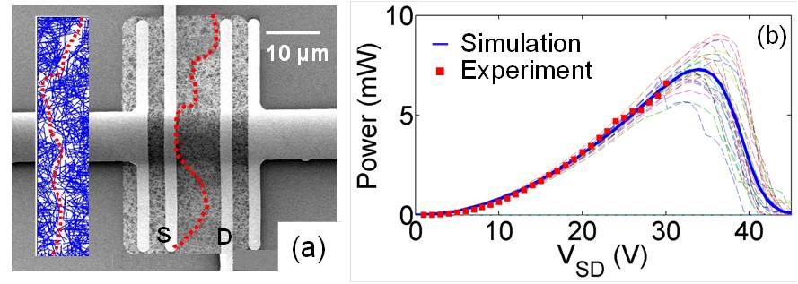 (a) Comparison of random CNT network from simulations (left inset, channel region) with scanning electron microscopy (SEM) image of the CN-TFT used in experiments after the breakdown, respectively. The red dotted line shows the breakdown pattern of the network. (b) Comparison of computational results to experimental measurements of dissipated power vs. source-drain voltage; the dark blue curve shows the statistical average of 50 random networks (dashed curves) obtained from the simulations.
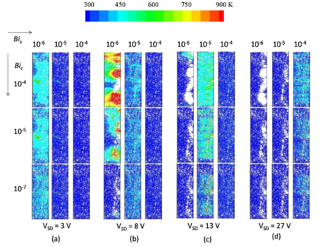
Temperature profile in CNT networks for different values of thermal contact conductances at CNT junction (BiC) and CNT-substrate interface (BiS) at different source to drain voltage (VSD) (a) 3 V, (b) 8 V, (c) 13 V, (d) 27 V. Network density = 3.5 CNTs/µm2. In each case the current flows from left to right (source to drain) of the panels, respectively. High voltage leads to excessive heat dissipation leading to breakdown of the CNT network. |
|
Relevant Publications: 1. Gupta, M. P., Behnam, A., Lian, F., Estrada, D., Pop, E., and Kumar, S., “High Field Breakdown Characteristics of Carbon Nanotube Thin Film Transistors,” Nanotechnology, 24 (40), 405204 2013. [PDF] 2. Gupta, M. P., Liang, C., Estrada, D., Behnam, A., Pop, E., and Kumar, S., “Impact of Thermal Boundary Conductances on Power Dissipation and Electrical Breakdown of Carbon Nanotube Network Transistors,” Journal of Applied Physics, 112, 124506, 2012. [PDF] 3. Kumar, S., N. Pimparkar, Murthy, J. Y., and Alam, M. A., “Self-consistent Electrothermal Analysis of Nanotube Network Transistors,” Journal of Applied Physics, 109, 014315, 2011. [PDF] 4. Kumar, S., Murthy, J. Y., and Alam, M. A., Percolating Conduction in Finite Nano-tube Networks, Physical Review Letters, 95, 066802, August 2005. [PDF]
Funding: NSF
|
|