Projects > AlGaN/GaN based high electron mobility transistors
|
|
AlGaN/GaN based high electron mobility transistors (AG-HEMTs) are the strong candidates for the high power and high frequency applications due to the superior properties ofAlGaN/GaN hetero-structure such as high carrier saturation velocity, wide band gap, high breakdown field and thermal conductivity. However, reliability concerns such as performance degradation at elevated temperatures or stresses need to be addressed for the widespread realization of AG-HEMTs. Understanding the underlying details of the thermal transport in the device is going to be an important step towards solving heat dissipation and reliability challenges in these devices. We develop a multi-scale diffuse-ballistic thermal transport model of AG-HEMTs and investigate the hot spot formation and energy transport from hot-spot. Device is studied under both DC and AC operations to understand the heat dissipation effects on device performance under realistic conditions.
|
|
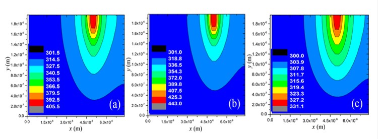
Figure 4. Spatial variation of (a) Longitudinal acoustic (LA) phonon temperature (b) Longitudinal optical (LO) phonon temperature; both from BTE and (c) temperature from Fourier model under the same volumetric heating source. Fourier model underestimates the device temperature. Temperatures are Kelvin.
|
|
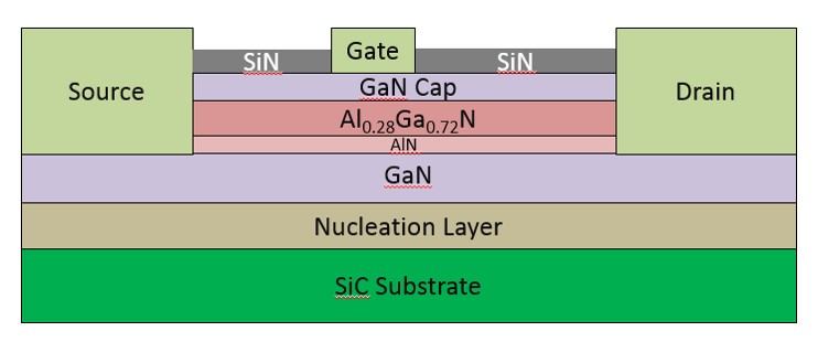
 Figure 2.
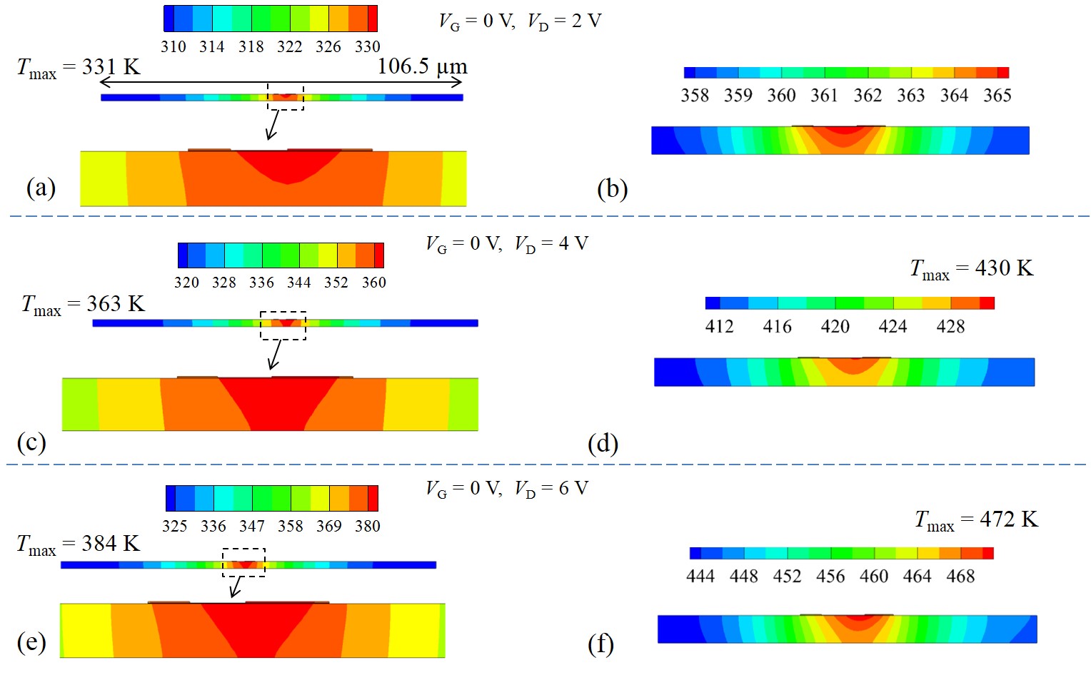 |
Figure 5. Effect of lateral thermal spreading on temperature profile of GaN layer. Figures on the left side (a, c, e) correspond to total lateral dimension of 106.5 µm and figures on the right (b, d, f) correspond to 26.5 µm. Channel length in both cases is kept the same at 6.5 µm. The epicenter of hot spot is located below the gate edge near drain. Bottom of substrate layer is kept at 300 K. Clearly in case of greater lateral dimensions temperature is lowered significantly (e.g., nearly 90 K at drain bias of 6 V (e, f)) |